


QUALITY STANDARDS





STAY UPDATED
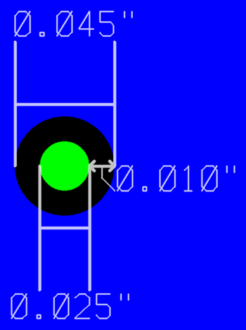
Inner layer clearances refer to the amount of empty space between a drill hit and unconnected copper on an inner layer. It acts as a buffer zone to ensure no connection is made.
For our standard services we require that all drill hits have a clearance at least 0.020" larger than the intended finish size of the hole. This size accounts for things like positional tolerance and plating allowance. Please see the example below.
Not all inner layer clearances are defined the same way in every CAD suite however. Some software uses a global setting, others require different settings for copper pours, traces, drill hits, etc.
We provide Design Rules for some common CAD suites on our website which can be useful as a verification process. From our CAD Tools Page look for your CAD Suite in the navigation menu. Most modern CAD suites do provide basic DFM utilities for verifying clearances however.
Our PCB123 Design software also includes a built in Design Rules Check (DRC) for our service which can be found under the Design menu or it can be run by simply pressing D on your keyboard.
If your order was placed on hold due to inner layer clearance violations there are a few options going forward:
If traces are causing the clearance violations they may need to be rerouted to achieve the required clearance.
 Get Quote